MDTLC Application Examples
Wire Over Plane
Wire Over Plane Impedance
Introduction
After a printed circuit board has been fabricated and assembled and is being tested, or sometimes even just after the design files have been irrevocably released for fabrication, a requirement to change one of the connections between components appears. This is done using a wire resembling wire-wrap wire. There are many names for this undesirable modification such as a strap, a blue wire, or a barnacle.
Just what is the transmission line impedance of this wire? Of course that depends on the wire and the surface over which it is run. Generally, it can be difficult to run a wire over a continuous copper plane, and some boards do not copper fill the outside layers. But for the purposes of this example, a ground fill plane is available on the top or bottom layer.
Conditions
- 30 AWG wire with 6.25mil thick Kynar insulation having an Er of 6.6. (Part number KYN30 MIL-W-81822)
- Solder mask coasting 1 mil thick with Er of 3.5.
Method
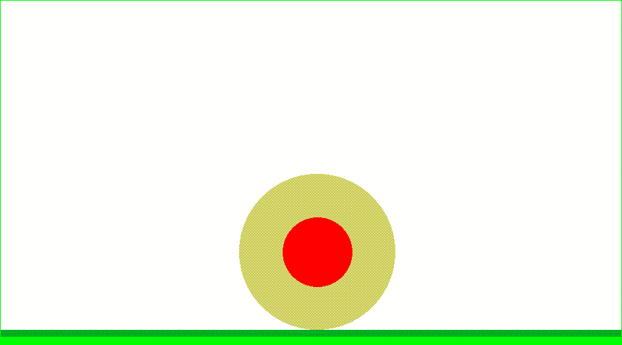
- A bit map was created using paint.net. The default paint program could have been used, but paint.net supports image layers. By drawing the plane on one layer, and the wire on the other layer, the wire can be “moved” before the image is flattened into a regular bitmap image.
- The colors used in the bitmap must match exactly the colors used for MDTLC internal bitmaps. MDTLC bitmaps can be exported and used as the basis to build a new bitmap. Note that all current versions appear to have a bug which does not allow a large bit map to be exported.
- Resize the bitmap so that the wire is 3 or 4 times away from every side except the ground plane side. Before doing this, set the bottom center as anchor. 500x900 pixels was used here. MDTLC default pixel size is 0.1mil/pixel, but except for the DC resistance value, any scale could be used.
- Add a layer above for drawing the wire.
- When using paint.net, turn anti—aliasing off.
- Use one of the laminate color values for the wire insulation. The wire core must be pure red.
- As of version 2.1.88, the RGB value for air is 255,255,254.
- Top solder mask RGB is {0x00,0xaf,0x1f} or 0,175,31
- The laminate 1 dielectric RGB is {0xc8,0xc8,0x64} or 200,200,100
- The laminate 2 dielectric RGB is {0xc8,0xc8,0x65} or 200,200,101
- Finally, ensure that the outside perimeter of the image is surrounded by a ground. Set paint.net to draw a 1 pixel width no-fill box, select green, and draw all around the perimeter.
- When running mdtlc, set the associated dielectrics with the desired Er values.
Test Cases
- Two calculations are run: one with the wire just touching the board surface, and the other with the wire 2 mil above the surface. This might be the case where tape holds the wire in place approximately every inch.


Results
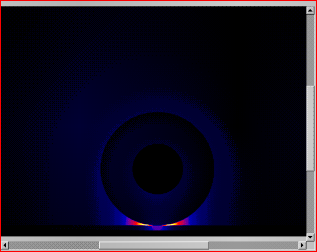
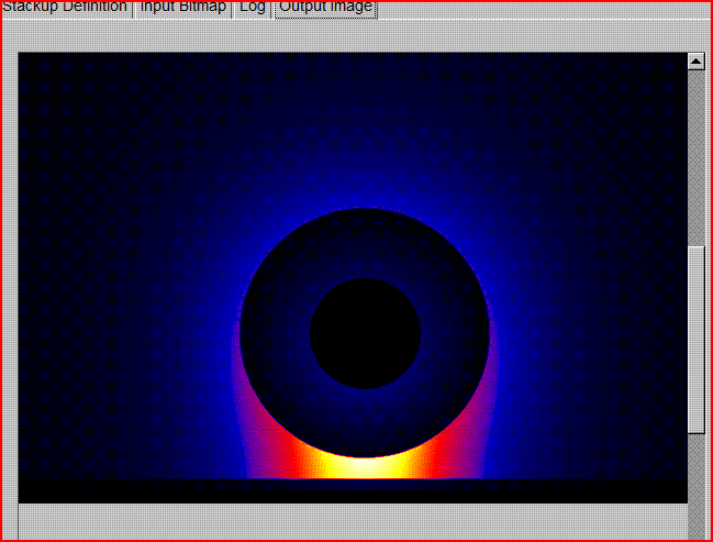
- With the wire on the solder mask, Zo=46.6ohms. With the wire 2 mil above, calculated Zo=61.3ohms. Note that the perimeter ground box lowers the impedance slightly.
- The program output and images are listed below.
-------------------------------
2D Impedance
Calculator Program
Version 0.2.1.88
Time: Fri Feb 22
07:04:17 2008
GPL Version 2.0
-------------------------------
Simulation pix map
150 pixels high by 700 pixels wide.
316024 bytes
allocated for bmp.
Reading file
C:/Dev-Cpp/development/trimp/wire-flat-bigger.bmp ...
Image pixel dimensions:
500 high x 900 wide
INPUT PARAMETERS:
Layer Thick Specifications
Solder Mask Top 1.00
Opening w=0.0 offset=0.0
Copper Plane Top 1.30
Opening w=0.0 offset=0.0
Laminate Layer 1 5.00
Resin Content 64.3% 3.2-6.0
Signal Layer 1 1.35
4.0-6.0-4.0 Etchback=0.00
Laminate Layer 2 5.00
Resin Content 64.3% 3.2-6.0
Copper Plane Bottom 1.30
Opening w=0.0 offset=0.0
Layer Thick Er
Loss Tangent
Solder Mask Top 1.00
3.50 0.00200
Copper Plane Top 1.30
3.20
Laminate Layer 1 5.00
4.20 0.00120
Signal Layer 1 1.35
6.60 0.00120
Laminate Layer 2 5.00
4.20 0.00120
Copper Plane Bottom 1.30
3.20
DC
resistance by dimensions:
Rdc_trace_1= 125.69 Rdc_trace_2 = 125.69 milliohms/in 20C
DC resistance by pixel count:
Rdc_trace_1=
8.498 milliohm/in.
C
= 3.363 pF/in L =
7.315 nH/in.
Er
= 3.426 Loss_tan = 0.00073
Zo
= 46.640 Ohms Delay = 156.833 ps/in.
Log file save name:
mdtlc_08012225730.txt
Reading file
C:/Dev-Cpp/development/trimp/wire-flat-bigger-up2mil.bmp ...
Image pixel
dimensions: 500 high x 900 wide
INPUT PARAMETERS:
Layer Thick Specifications
Solder Mask Top 1.00
Opening w=0.0 offset=0.0
Copper Plane Top 1.30
Opening w=0.0 offset=0.0
Laminate Layer 1 5.00
Resin Content 64.3% 3.2-6.0
Signal Layer 1 1.35
4.0-6.0-4.0 Etchback=0.00
Laminate Layer 2 5.00
Resin Content 64.3% 3.2-6.0
Copper Plane Bottom 1.30
Opening w=0.0 offset=0.0
Layer Thick Er
Loss Tangent
Solder Mask Top 1.00
3.50 0.00200
Copper Plane Top 1.30
3.20
Laminate Layer 1 5.00
4.20 0.00120
Signal Layer 1 1.35
6.60 0.00120
Laminate Layer 2 5.00
4.20 0.00120
Copper Plane Bottom 1.30
3.20
DC resistance by dimensions:
Rdc_trace_1= 125.69 Rdc_trace_2 = 125.69 milliohms/in 20C
DC resistance by pixel count:
Rdc_trace_1=
8.498 milliohm/in.
C
= 2.110 pF/in L =
7.938 nH/in.
Er
= 2.333 Loss_tan = 0.00022
Zo
= 61.344 Ohms Delay = 129.408 ps/in.
E-Field Images

