Multiple Dielectric Transmission Line Calculator
History
· August 2007 – Initial Release. Tested and results found to be close to commercial calculators, but all different configurations have not been tested.
· 20 Dec 2007 – Updated web page to include features in version 0.2
Related Links
Introduction
Using the proven atlc code to provide the field solver, this transmission line calculator program provides a way to compute the transmission line characteristics of many common structures found in PCB board design. Transmission line characteristics computed include:
1. Differential odd mode impedance
2. Differential even mode (common mode) impedance
3. Odd mode dielectric constant (and propagation delay)
4. Even mode dielectric constant (and propagation delay)
5. Even and odd mode dielectric loss
6. Capacitance per unit length
7. DC resistance.
Mdtlc calculations can be slow in some cases (where the electric field is widely dispersed as in surface microstrip), but is adequate for occasional or educational use.
Description
Mdtl is a GUI based application that can run the win32 platforms. Transmission line impedance calculation is a common task in printed circuit board design, and this application provides the ability to model multiple dielectrics. This ability is not common among other calculators. One other open source calculator is atlc.
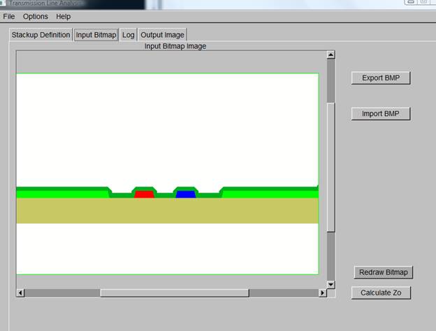
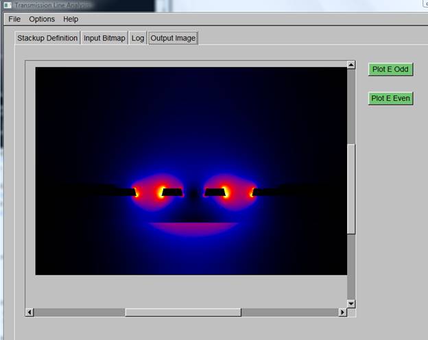
Atlc can compute the transmission line characteristics for an arbitrary cross section as defined by a bitmap. Initially developed as a *nix command line program, it provides nearly the ultimate in flexibility for describing the transmission line cross section. However, this format and flexibility increases the setup time needed to describe the physical characteristics of the transmission line. Mdtl builds on the atlc base to provide a GUI based interface that allows a quick way to describe structures common in printed circuit board (PCB) design. Mdtl takes the parameters used to describe the PCB structure, and generates the bitmap required for the atlc computation. Once the computation is complete, the results are displayed in the GUI.
Multiple dielectrics are supported in this approach to field solving. As such, it is possible to observe the propagation delay differences between single-ended and differential signals caused by different dielectric constants of glass and resin.
Additionally, impedances can be checked for unusual cases such as when the differential pair is close to the edge of the board.
Usage
The main panel provides basic inputs. If details like etchback or local dielectric values are required, then press the appropriate EDIT button.
Units are currently fixed to English system. 1 mil equals 0.001 inch.
Use the bitmap EXPORT and IMPORT functions with care. The color values in the bitmap are associated with the various dielectrics. The difference in the color map between LAMINATE 1 and LAMINATE 2 is one bit. Use the bitmap editors color picker to check the 24-bit colormap value. Using unknown colors will cause a crash.
The executable is a single binary – it does not install on the system. Any output files are written to the directory in which the executable is started. For example, if it is on the Desktop, output files are written to the desktop.
Output filenames have a fixed root name combined with a date and time number string.
Note that while it is possible to enter unbalanced differential structures, the output format of odd and even impedances does not fully describe the loading on a driver.
Pixels correspond to 0.0001 inches. Accuracy for copper thicknesses such as 1/8 ounce is likely affected.
Examples
Comparison to other calculators
|
|
Single Ended Surface Microstrip |
|||
|
Parameters |
Name |
Version |
Z (Zodd/Zeven) |
Propogation Delay (odd/even) |
|
No solder mask No etchback W = 6 Cu = 1.8 oz Er = 4.2 Laminate = 5mil |
mdtlc |
0.1.1.811 |
56.8 |
139.2 ps/in |
|
CITS25 |
2.0.2.0 |
58.4 |
|
|
|
Hyperlynx |
7.5 |
58.9 |
141.8 ps/in |
|
|
|
Single Ended Stripline |
|||
|
No etchback W = 6 mil Cu = 0.5 oz Er = 4.2 Laminate1=5 Laminate2=10 |
Mdtlc |
|
47.6 |
173.6 ps/in |
|
CITS25 |
|
47.15 |
|
|
|
Hyperlynx |
|
47.0 |
174.8 ps/in |
|
|
|
Differential Microstrip |
|||
|
No soldermask No etchback W1=W2 = 4 mil Spacing = 8 Cu = 1.4mil Er = 4.7 Laminate1=2.6 |
mdtlc |
|
93.4/24.8 |
144.2/149.5 ps/in |
|
CITS25 |
|
92.99 |
145.7 ps/in |
|
|
ADS |
|
88.8/25.1 |
147.7/159.7 ps/in |
|
|
Hyperlynx (from paper) |
|
87.2/26.0 |
145.1/154.9 ps/in |
|
|
|
Differential Embedded Microstrip |
|||
|
No soldermask Etchback 0.4 W1=W2 = 3 mil Spacing = 4 Cu = 1.4mil Er _lam= 3.8 Er_resin=3.2 Laminate1=2.5 Laminate2=19.7 |
mdtlc |
0.1.1.839 |
110.9/78.0 |
154.6/144.4 ps/in |
|
Polar Si6000 |
|
106.53 |
|
|
|
|
Differential Stripline |
|||
|
No soldermask No etchback W1=W2 = 4 mil Spacing = 8 Cu = 1.4mil Er = 3.25 Laminate1=12 Laminate2=12 |
mdtlc |
0.1.1.564 |
82.9/30.2 |
152.7 ps/in |
|
LineCalc |
|
84.2/30.0 |
|
|
|
CITS25 |
2.0.2.0 |
82.0 |
152.7 ps/in |
|
|
Hyperlynx |
7.5 |
82.2/30.2 |
|
|
Future Work
1. The solder mask drawing algorithm is not that good. Need to coat vertical surfaces as well.
2. Save and import configuration settings.
3. Save and import the bitmap file.
4. Compare results to known configurations.
5. Modeling the glass and resin composite – may require a 3D simulation or multiple 2D simulations.
6. More trace configurations (co-planar ground).
7. Ribbon cable and cable configurations possible.
8. Create a properly formatted output page (in pdf) including the bitmap.
9. Estimated breakdown strength of dielectric.
10. Modify inner loops to speed up simulation.
11. Incorporate multi-threading.
12. Change output report format to support unbalanced differential impedances.
13. Add dielectric loss.
14. Add current filament simulation for inductance simulation and skin effect loss values.
Screenshots


